
Last week, I attended the camLine Breakfast for Engineers in South Austin. Reconnecting with Bernardo Ospina, camLine’s Key Account Manager in the Americas and a former colleague from our LATAM days, was the highlight of the session! Discussing the “Ground Truth” of the shop floor with someone who understands the global stakes was a powerful reminder: in 2026, the distance between a “good” wafer and a “world-class” yield is measured entirely in Data Integrity.
I’ve spent Q1 advocating for “Quantitative Certainty”. In the high-velocity world of semiconductor manufacturing, that certainty is no longer a luxury—it is the only way to manage the components that define our daily lives.
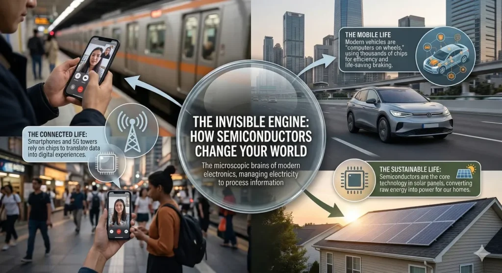
The Invisible Engine: How Semiconductors Change Your World

Semiconductors are the “brains” of modern electronics, acting as microscopic switches that manage electricity to process and transmit information. Without them, our modern existence would stall:
- The Connected Life: Smartphones and 5G towers rely on chips to translate data into the digital experiences we rely on daily.
- The Mobile Life: Modern vehicles are “computers on wheels,” using thousands of chips for engine efficiency and life-saving braking systems.
- The Sustainable Life: Semiconductors are the core technology in solar panels, converting raw energy into power for our homes.
The Big Three: America’s Semiconductor Powerhouses
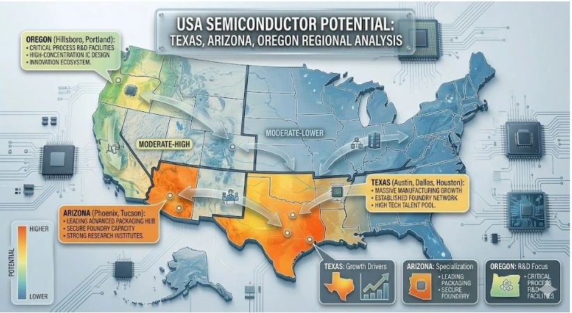
As we navigate the $975 billion global chip market of 2026, the U.S. has solidified three primary hubs that drive our domestic “Silicon Shield.”
1. Texas: The Beating Heart of the Silicon Hills
Right here in Austin, we are witnessing a manufacturing explosion. Texas leads the nation in semiconductor exports—a position it has held for 14 consecutive years—and is a top state for semiconductor employment with a workforce of more than 51,500 Texans. With major expansions from Samsung, Texas Instruments, and NXP, Austin has become the central node for “Integration Integrity”—the difficult task of merging legacy facilities with brand-new, AI-driven greenfield operations. Samsung’s $17 billion Taylor facility is on track to be operational by late 2026.
2. Arizona: The Silicon Desert
Arizona remains a titan for leading-edge logic. With multiple mega-fabs from TSMC and Intel under construction, the state is set for one of the strongest multi-year manufacturing booms in the country. TSMC’s Phase 1 facility in North Phoenix reached a 92% yield rate for its 4nm process by late 2025. The “Guardrail” in the desert is Resource Stability; when your margin for error is measured in nanometers, environmental fluctuations must be tracked with surgical precision, especially as Intel ramps up its 18A process node.
3. Oregon: The R&D Powerhouse
Oregon remains the nation’s R&D titan, anchored by Intel’s research facilities in Hillsboro, the company’s largest site globally. The focus here is Yield Velocity—the speed at which a new chip design moves from the lab to high-volume manufacturing. Intel’s D1X development factory is currently using the world’s first high-numerical aperture EUV lithography tool to maintain leadership through 2026. This ensures errors are caught before high-volume production begins.
The Nerve Center: Why MES is the Ultimate Guardrail
In a fab, a single wafer undergoes over 1,000 process steps. As Bernardo and I discussed, the Manufacturing Execution System (MES) is the “Nerve Center” that prevents catastrophes.
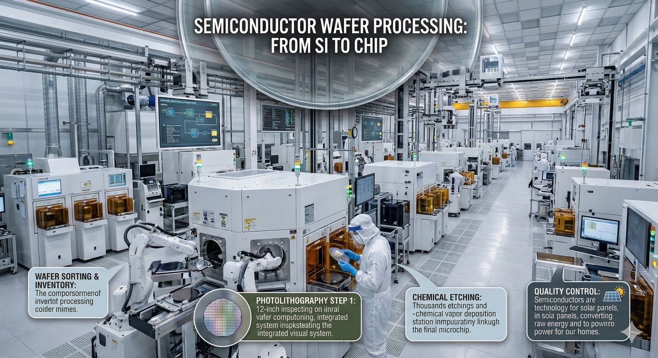
- Real-Time Visibility: MES provides real-time monitoring across wafer processing, achieving equipment utilization rates above 90%.
- Yield Optimization: As we move toward 3nm nodes, the margin for error vanishes. MES solutions provide Statistical Process Control (SPC) that keeps defect rates below one part per million.
- Global Knowledge Sharing: Just as Bernardo and I shared insights across borders in LATAM, camLine’s platform ensures that a lesson learned in an Oregon lab is instantly applied to an Austin fab (Brynjolfsson & McElheran, 2016).
March Mandate: Implementing Quantitative Certainty
As we close out Week 10 of 2026, the “New Year adrenaline” has faded into the hard reality of execution. Whether you are in Austin, Phoenix, or Hillsboro, your mandate for March is to Eliminate the Autopsy.
- Audit Your Latency: Define a “Max Wait Time” for wafer handoffs.
- Verify System Integration: Ensure your MES and ERP are speaking the same language.
- Prioritize Ground Truth: Like my exchange with Bernardo, encourage your engineers to flag anomalies early. Vulnerability is a risk mitigation strategy, not a weakness (Senge, 1990).
A Note of Gratitude
As I look toward 2026, I am filled with gratitude for the community that makes this innovation possible. A special thank you to the camLine team for the invitation to the Breakfast for Engineers. It was a privilege to witness first-hand why your solutions remain a leader in the semiconductor space, providing the Quantitative Certainty that modern manufacturers demand.
Most importantly, I want to thank Bernardo Ospina. Reconnecting with a former colleague from our LATAM days was a powerful reminder that while technology changes, the value of Accountability and Integrity is timeless. Thank you for the insightful session and for continuing to push the boundaries of what is possible in the Silicon Hills!
Myriam Hernández Múzquiz specializes in channel partnership strategy and operational excellence. With a background in managing large-scale CRM operations, she helps organizations build revenue-driving partner ecosystems.
References
Brynjolfsson, E., & McElheran, K. (2016). The rapid adoption of data-driven decision making. American Economic Review, 106(5), 133-139.
Intel Newsroom. (2025). Intel’s Oregon Investments Fuel US Silicon Innovation Leadership.
Office of Governor Greg Abbott. (2026). Texas Semiconductor Leadership.
Samsung Semiconductor Global. (2026). Building a Bright Future at Our Taylor, Texas Fab.
U.S. Department of Commerce. (2025). How Semiconductors Power Our Lives.
Editor’s Note: This article was reviewed and refined with the assistance of Google’s Gemini.